Industrial CT
Industrial CT technology is the abbreviation of Industrial Computed Tomography, which was proposed by Randon J in 1917 and was not applied in nondestructive testing until 1970s. As the advancement of computer science and the development of detector technology booming, industrial CT has been improving significantly in recent years, which has widely used in aerospace, nuclear, military, as well as in manufacturing for non-destructive mapping and layered design and manufacturing. Industrial CT, a practical nondestructive testing method, is developing from the low-energy industrial CT that meets the general industrial application to the high-energy field that meets the testing requirements of large and complex structural parts.
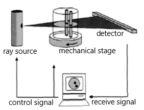
Radiation detection server as the foundation of industrial CT. When the collimated beam of energy I0 passes through the object, the attenuation coefficient μi of each volume element in each transmission direction is different. As a result, the transmitted energy I received by the detector is also different. According to a certain image reconstruction algorithm, a thin section of the section of the inspected workpiece without image overlap can be obtained (Fig.1), and a new tomography image can be obtained by repeating the above process. When enough two-dimensional tomography images are measured, three-dimensional images can be reconstructed.
In fact, industrial CT is a ray-detection technology. Compared with conventional ray-detection technology, the main advantages of industrial CT are as follows:
- The image target of industrial CT is not blocked by the surrounding details. The feature of the target, such as spatial position, shape and size information, can be obtained directly.
- Industrial CT has outstanding density resolution ability, and the density resolution of high-quality CT image can reach 0.1% or even higher.
- industrial CT images are the results of digitization, which are convenient for storage, transmission, analysis and processing.
In industrial CT, X-ray sources are commonly used in X-ray machines and linear accelerators. There are three kinds of detectors commonly used: high resolution CMOS semiconductor chip, flat plate detector and scintillation detector. Flat panel detectors are typically made of amorphous silicon or amorphous selenium covered with scintillation crystals of several hundred microns, such as CsI, with pixel sizes of about 127 microns and image quality close to that of film. The advantage of scintillation detector is high detection efficiency, especially in high energy conditions, it can reach the dynamic range of 16 ~ 20 bits and read speed in the order of microseconds.
Detector is one of the core components of industrial CT system, which has great influence on the quality of reconstructed images. The following performance indexes should be considered in the design of detector: detection efficiency, linearity, dynamic range, uniform consistency, stability, size, response speed, number of channels, etc.
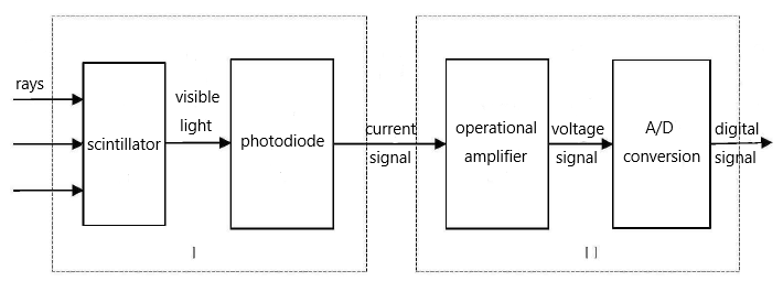
The signal conversion process of industrial CT detector can be clearly seen from the detector structure diagram (Fig.2). First, the ray signal enters the scintillator, where visible light is generated. Photodiodes convert visible light into current signals. Then, the i-v conversion circuit converts the current signal into a voltage signal. Finally, it is converted into digital signal by AD conversion device and transmitted to data transmission system.
From the description of the structure of scintillator detector, it can be seen that its working principle is as follows: when the ray enters the scintillator, secondary electrons are generated at a certain point, which ionize and excite the molecules or atoms of the scintillator and emit a large number of photons in the deexcitation. Due to the effect of the reflective layer around the scintillator, a large part of the fluorescence reaches the photosensitive surface of the photodiode through the photocoupling agent or optical guide. Photodiodes convert optical signals into current signals, and then convert and amplify them through subsequent circuits to output voltage signals that can be measured. To sum up, the working process of scintillator detector can be divided into the following stages:
(1) the ray enters the scintillator and interacts with it. The scintillator absorbs part of the ray energy to excite and ionize molecules, so energy deposition rate exists.
(2) when excited molecular deexcitation occurs, part of the energy is used for fluorescence; The other part of energy is converted into thermal motion, which heats up the scintillator, so the scintillator has absolute scintillation efficiency.
(3) collect as much fluorescence as possible on the photosensitive surface of the photodiode by using reflective materials. In this process, some photons will be absorbed or escape from the scintillator, so there will be light collection efficiency problems.
(4) after the fluorescence enters the p-junction of photodiode, the electron-hole pair is excited. Under the action of internal potential field or external bias voltage, the electrons and holes move to the poles respectively to form photocurrent, and the photocurrent is proportional to the light intensity.
An ideal scintillator crystal should have the following characteristics :
- it should have high luminous efficiency to convert the energy of radiation into detectable optical signals.
- the transformation process from ray to fluorescence is linear, that is, the number of photons produced should be proportional to the energy of scintillator deposition as far as possible.
- there must be good light collection efficiency, and the scintillator should be transparent to the light it emits.
- the scintillator shall have good optical properties and be made to meet the size required by the actual detector.
(5) the refractive index of the scintillator material should be similar to that of silicon, so that the fluorescence can be effectively coupled to the photosensitive surface of the photodiode array.
In fact, all existing scintillator materials cannot meet all the above characteristics at the same time. Therefore, the most suitable scintillator materials should be selected according to the practical application requirements. Currently, CsI(TI), BGO and CdWO4 are the most widely used inorganic scintillators in industrial CT and the scintillation properties are shown in Table 1. These kinds of scintillators are introduced respectively below.
Scintillation characteristics of CsI(Tl), BGO and CdWO4
| properties | CsI(Tl) | BGO | CdWO4 |
| Light yield (photos/MeV) | 52000 | 8500 | 13000 |
| Peak wavelength (nm) | 550 | 480 | 515 |
| Density (g/cm3) | 4.5 | 7.13 | 7.9 |
| Radiation length (cm) | 1.86 | 1.12 | 1 |
| Melting point (℃) | 621 | 1050 | 1123 |
| Refractive index ( peak wavelength) | 1.78 | 2.25 | 2.15 |
| Decay time (ns) | 1000 | 300 | 20000 |
| Light yield coefficient (%/℃) | 0.32 | -1.6 | 0.1 |
Scintillation crystals used in Industrial CT
CsI
| Wavelength (Max. Emission) (nm) | 410 |
| Decay time (ns) | 40 |
| Light yield (Photons/kev) | 25 |
| Light output relative to Nal (TI) (%) | 75 |
| Refractive index | 1.82@410nm |
With the development of nuclear technology and high energy physics, the application of inorganic scintillation crystal has been expanded, and the requirements for inorganic scintillation crystal are higher and higher. As early as the 1980s, the advantages of CsI (Tl) crystals were noted: emission spectra could be matched to silicon photodiodes, optical emissivity was high, irradiation length was shorter than NaI (Tl) crystals, and mechanical properties were good. An excellent and useful scintillation crystal material. In recent years, the crystal has been favored for its improved radiation resistance. With the development of nuclear technology and high energy physics, the application of inorganic scintillation crystal has been expanded, and the requirements for inorganic scintillation crystal are higher and higher. As early as the 1980s, the advantages of CsI (Tl) crystals were noted: emission spectra could be matched to silicon photodiodes, optical emissivity was high, irradiation length was shorter than NaI (Tl) crystals, and mechanical properties were good. An excellent and useful scintillation crystal material. In recent years, the crystal has been favored for its improved radiation resistance.
The CsI (Tl) scintillator emits up to 52,000 photons/MeV, and the peak wavelength of the emission spectrum is 550nm, which matches the response spectrum of silicon photodiode. Its decay time consists of 0.6 US for the fast component and 3.5 Us for the slow component. In addition, CsI (Tl) scintillators have high mechanical strength, strong impact and vibration resistance, and strong plasticity, making them easy to process into thin sheets. Compared with NaI (T1) scintillator, CsI (Tl) scintillator has better performance than NaI (Tl), but its luminescence efficiency is lower than NaI (Tl) : it is not soluble, has a large ray absorption coefficient, and the volume can be relatively small. The peak wavelength is 565nm, which is well matched with silicon photodiode. Therefore, CsI (Tl) scintillators are commonly used in low-energy industrial CT.
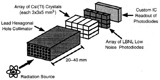
The diagram illustrates the module of a discrete flicker camera. The prototype features a 3×4 pixel array, each pixel consisting of a 3×3 ~ 5 mm3 CsI (TI) crystal coupled to a 3×3 mm2 PIN photodiode. The readout circuit consists of two 3×3 mm2 ics. Cameras with useful imaging sizes can be constructed from arrays of single modules.
References
[1] Csl(Tl)-Calorimeter Calibration with Positive-Kaon Decay Products
[2] Study of the growth atmosphere effect on optical and scintillation characteristics of large CsI(TI) crystals
[3] A Discrete scintillation Camera Module Using Silicon Photodiode Readout of CsI(T1) Crystals for Breast Cancer Imaging
[4] Light response and particle identification with large CsI(T1) crystals coupled to photodiodes
[5] New Limits on Interactions between Weakly Interacting Massive Particles and Nucleons Obtained with CsI(Tl) Crystal Detectors
[6] Limits on Interactions between Weakly Interacting Massive Particles and Nucleons Obtained with CsI(Tl) Crystal Detectors
BGO
| Wavelength (Max. Emission) (nm) | 480 |
| Decay time (ns) | 300 |
| Light yield (Photons/kev) | 8-10 |
| Refractive index | 2.15 |
| Energy resolution (%) | 12 |
Scintillation can effectively convert high-energy particles and radiation into light at wavelengths in or around the visible spectral region, which is widely used in nuclear medicine imaging, industrial CT and high-energy physics. Bismuth germanate (Bi4Ge3O12 or BGO) is an excellent scintillator developed in 1975. It has been widely studied because of its interesting luminescence properties, such as short attenuation time in visible band, illumination, radioluminescence and two-photon absorption under high power laser. Its biggest advantage is its high atomic number and density (7.138/cm3), so it has a large absorption coefficient for both low energy and high energy rays, and high detection efficiency. Its emission spectrum ranges from 350nm-650nm, and its peak wavelength is about 480nm. In addition, it also has the advantages of good transparency, short luminescence decay time, and not easy to mature. However, its disadvantage is that its luminescence efficiency is low, which is only 14% of that of NaI (Tl) commonly used in high-energy industrial CT.
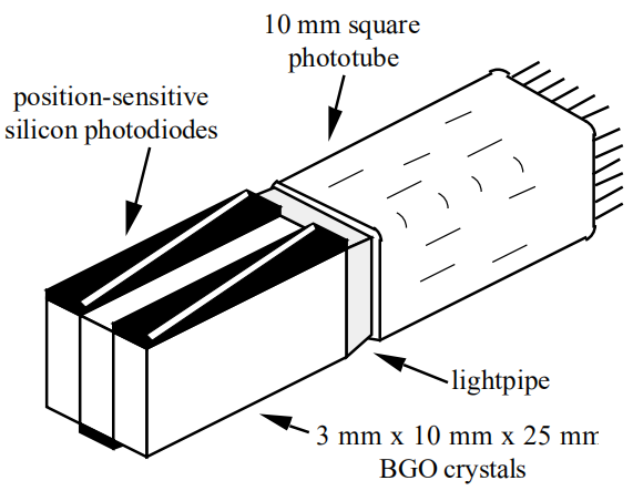
A detector consisting of three or more optically isolated BGO crystals attached to a 10 mm square photomultiplier tube that provides a fast timing pulse to the group is shown. Each crystal is also individually coupled to a position-sensitive photodiode that identifies crystals that prevent the annihilation of photons and determines the depth of the interaction.
References
[1] Synthesis and characterization of BGO with different chelating compounds by the polymeric precursor method, and their effect on luminescence properties
[2] INITIAL CHARACTERIZATION OF A POSITION-SENSITIVE PHOTODIODEBGO DETECTOR FOR PET
[3] Calibration and irradiation study of the BGO background monitor for the BEAST II experiment
[4]High Light Response Uniformity in Industrial Growth of 600-mm-Long BGO Crystals for DArk Matter Particle Explorer
[5] Study of the gamma spectrum of 16N with a BGO detector, for the purpose of calibration and of determining the fluorine grade of mineral samples
[6] Radiation tolerance studies on the VA32 ASIC for DAMPE BGO calorimeter
[7] Readout system for groundbased tests of BGO calorimeter of DAMPE satellite
[8] Nonlinear Absorption Response Correlated to Embedded Ag Nanoparticles in BGO Single Crystal From Two-Photon to ThreePhoton Absorption
[9] Simulation study of BGO array for characteristic gamma rays from neutronstimulated elements
[10] A system for low-level the cosmogenic 22Na radionuclide measurement by gamma–gamma coincidence method using BGO
CdWO4
| Wavelength (Max. Emission) (nm) | 490 |
| Decay time (ns) | 14000 |
| Light yield (Photons/kev) | 12-15 |
| Light output relative to Nal (TI) (%) | 50 |
| Refractive index | 2.2-2.3 |
Chromium tungstate scintillator (CdWO4) has the advantages of no moisture, high density, large X-ray absorption coefficient, short radiation length and resistance to radiation damage. In addition, the emission spectrum of CdWO4 scintillator is in the range of 400nm-600nm, and the emission peak wavelength is about 515nm, which can well match the sensitive wavelength of photodiode. CdWO4 scintillators have excellent scintillation properties and are the best in the tungstate series. Because of these advantages, CdWO4 scintillators are very suitable for high-energy industrial CT detectors, while CdWO4 crystals can make the detector very compact, thus improving the spatial resolution of the CT system. The excellent scintillation and optical properties of CdWO4 crystals make them widely used in high-energy industrial CT detectors.
With the continuous improvement of reliability and safety requirements of large parts, monitoring the assembly quality changes of parts has become a key technology to ensure safety. To solve the above problems must rely on industrial CT, especially high energy industrial CT terminal can be well realized. Therefore, the use of industrial CT technology, especially high-energy industrial CT technology, is expected to solve the following technical problems:
- (1) Precision test the welding quality of special parts.
- (2) Monitor assembly quality of large parts (such as part pose, assembly clearance and position variation) and precision inspection of internal structure.
- (3) Structural simulation and industrial CT examination of other materials and components.
References
[1] Size effects on the properties of high z scintillator materials
[2] Low thermal gradient Czochralski growth of large CdWO4 crystals and electronic properties of (010) cleaved surface
[3] Growth Defect W3+-W2+ of CdWO4 Crystals
[4] Preparation, structural and optical properties of ZnWO4 and CdWO4 nanofilms
[5] Multi-mode photocatalytic performances of CdS QDs modified CdIn2S4CdWO4 nanocomposites with high electron transfer ability
[6] Photoluminescence Studies and Core–Shell Model Approach for Rare Earthdoped CdWO4 Nano Phosphor
[7] Systematic Control of Monoclinic CdWO4 Nanophase for Optimum Photocatalytic Activity